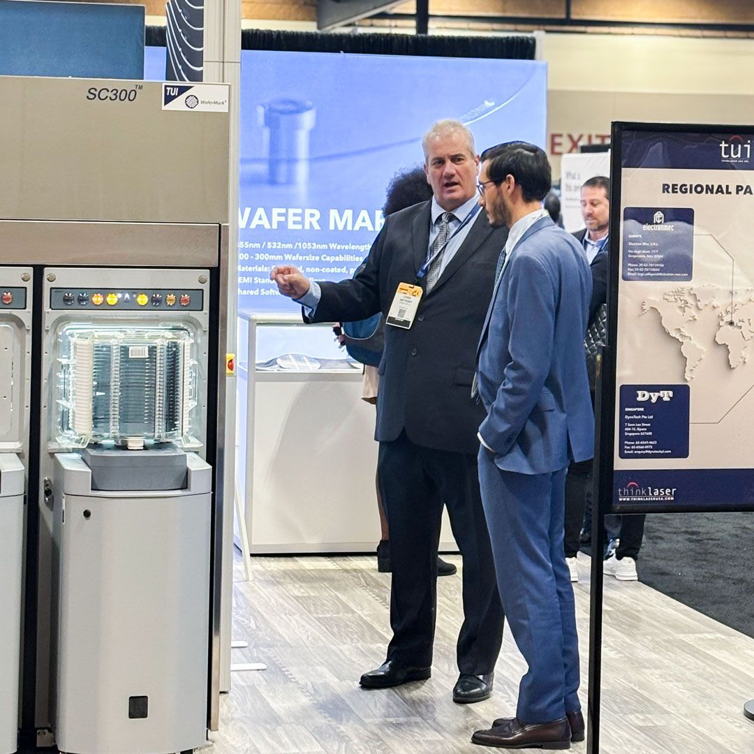
For more than 30 years, Thinklaser USA has been committed to developing innovative wafer marking solutions that help semiconductor manufacturers improve efficiency, accuracy, and productivity. As the industry continues to evolve, our engineering team remains focused on delivering technologies that address the growing demands of advanced semiconductor manufacturing.
Over the past several years, Thinklaser USA has introduced numerous innovations designed to improve throughput, expand material compatibility, and streamline wafer handling processes.
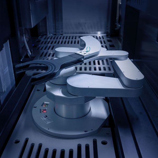
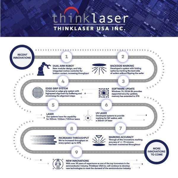
One of the most significant advancements has been the development of our dual-arm robotic platform. Featuring a new modular design and fully integrated motion controller, this system increases throughput by optimizing bottom-contact wafer handling while maintaining the precision our customers expect.
We have also developed backside wafer marking technology utilizing folding optics, allowing wafers to be marked on the back side without requiring the wafer to be flipped. This innovation reduces handling complexity while improving process efficiency.
As semiconductor materials continue to diversify, Thinklaser USA has expanded its laser capabilities to support 355nm UV, 532nm green, and 1053nm infrared laser platforms. These technologies provide customers with greater flexibility when marking a wide range of wafer materials and applications.
To support the growing adoption of silicon carbide (SiC) and other advanced substrates, we developed UV laser marking systems specifically designed for transparent and challenging wafer materials. These systems enable high-quality marking while preserving material integrity.
Additional innovations include enhancements to our edge grip system, which utilizes high-speed alignment and buffering techniques to minimize alignment steps and improve overall system performance. Combined with software upgrades supporting modern Windows operating systems, expanded memory capacity, and enhanced security updates, these improvements help customers maximize system reliability and productivity.
Perhaps most importantly, while implementing these advancements, Thinklaser USA has maintained marking accuracy of ±75 microns across our systems. At the same time, throughput improvements of up to 50% have been achieved on multiple platforms, helping customers meet increasing production demands without sacrificing quality.
Innovation has always been a cornerstone of Thinklaser USA’s success. As semiconductor technologies continue to advance, our team remains dedicated to developing next-generation wafer marking solutions that help manufacturers improve traceability, automation, and manufacturing efficiency.
The past several years have brought exciting advancements, and we believe the future holds even greater opportunities. More innovations are already in development as we continue to support the evolving needs of the global semiconductor industry.