
Precision UV Laser Marking for Semiconductor Wafers

As semiconductor devices continue to become smaller and more complex, manufacturers require wafer marking solutions that deliver exceptional precision without compromising delicate wafer surfaces. UV laser marking technology has become a preferred solution because it combines high-resolution marking capabilities with minimal thermal impact, making it well suited for advanced semiconductor manufacturing environments.


Unlike longer wavelength laser systems, UV lasers operate at shorter wavelengths that allow energy to be absorbed more efficiently by many semiconductor materials. This enables clean, high-contrast marks while reducing the heat transferred to the surrounding area. The result is precise wafer identification with minimal heat-affected zones, helping preserve wafer integrity throughout the manufacturing process.


Reliable wafer traceability is essential at every stage of semiconductor production. From process monitoring and quality control to inventory management and final device verification, permanent and readable wafer markings provide manufacturers with the confidence that every wafer can be accurately identified throughout its lifecycle.


ThinkLaser USA's WaferMark® laser marking systems are engineered specifically for semiconductor applications, delivering the precision, repeatability, and reliability required by today's fabrication facilities. Designed to meet demanding production requirements, WaferMark® solutions help manufacturers achieve consistent marking performance while supporting long-term process stability.


Advantages of UV Laser Wafer Marking

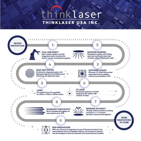
  • High-resolution laser marking for fine features, 2D Data Matrix codes, and alphanumeric identification
  • Minimal thermal impact to help protect sensitive wafer materials
  • Excellent mark contrast for improved readability and automated inspection
  • Permanent wafer identification that supports complete manufacturing traceability
  • Compatibility with a broad range of semiconductor materials and wafer applications
  • Reliable, repeatable performance for high-volume production environments

As semiconductor manufacturing continues to advance, traceability requirements are becoming increasingly important. Selecting the right laser marking technology can improve process consistency, support quality initiatives, and enhance overall manufacturing efficiency.


With decades of experience serving the semiconductor industry, ThinkLaser USA continues to develop laser marking solutions that help manufacturers meet today's production challenges while preparing for tomorrow's technology demands.


Learn more about ThinkLaser USA's WaferMark® semiconductor laser marking systems and discover how our UV laser technology can support your wafer marking and traceability requirements by calling or emailing a sales representative today.


Related Posts

Why Customer Support Matters in Industrial Laser Technology

Why Customer Support Matters in Industrial Laser Technology

We are excited to share that Thinklaser USA Investing in a laser marking or laser processing system is about more than purchasing...

Innovations Driving the Future of Semiconductor Wafer Marking

Innovations Driving the Future of Semiconductor Wafer Marking

For more than 30 years, Thinklaser USA has been committed to developing innovative wafer marking solutions that help semiconductor...

Semiconductor Review: Thinklaser USA Discusses the Future of Wafer Marking

Semiconductor Review: Thinklaser USA Discusses the Future of Wafer Marking

We are excited to share that Thinklaser USA was recently featured in Semiconductor Review, where our President, Chris Anthony...