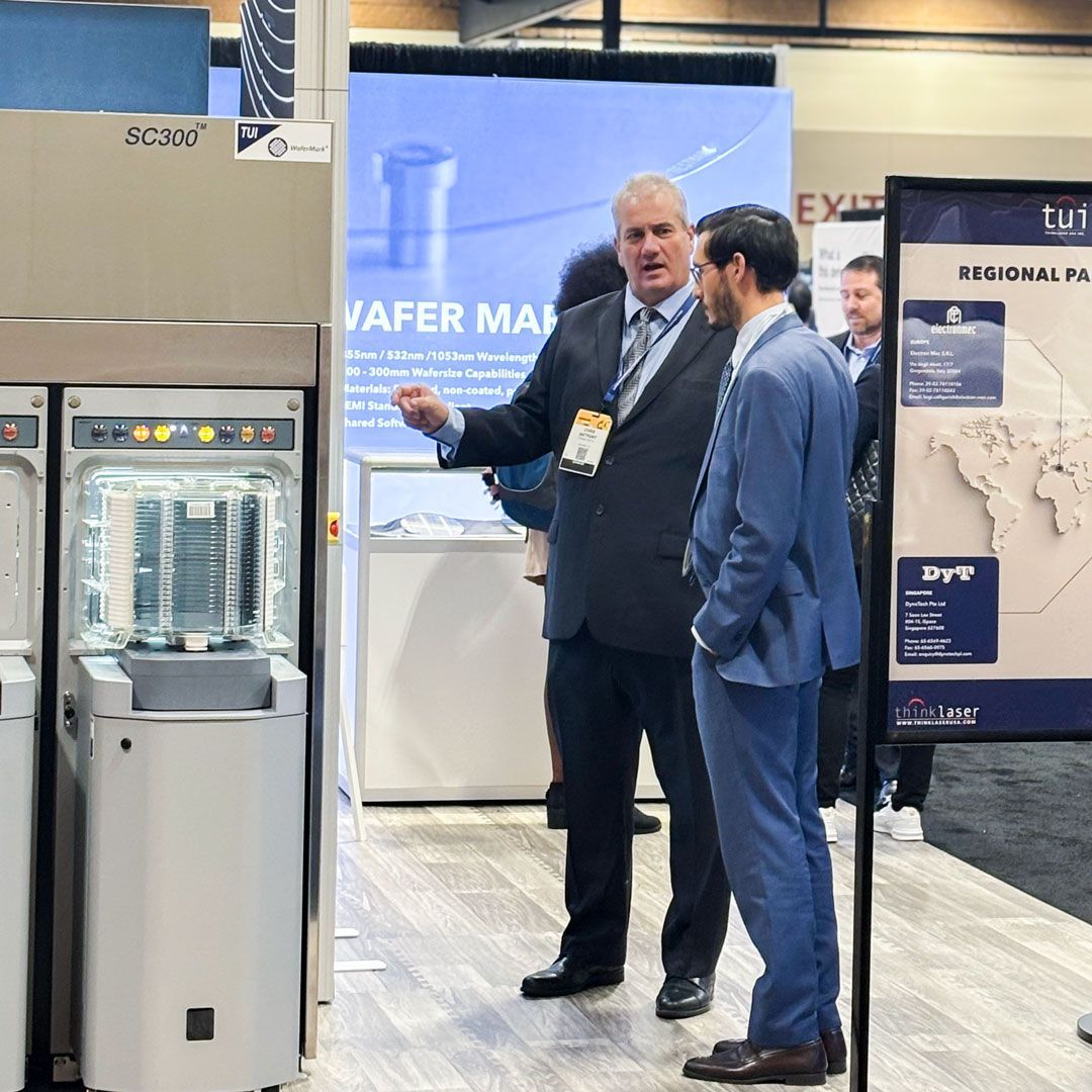
We are excited to share that Thinklaser USA was recently featured in Semiconductor Review, where our President, Chris Anthony, discussed the company’s role in advancing wafer marking technology for the semiconductor industry.
The interview highlighted our ongoing commitment to helping semiconductor manufacturers improve wafer traceability, process control, and production efficiency through innovative laser marking solutions.
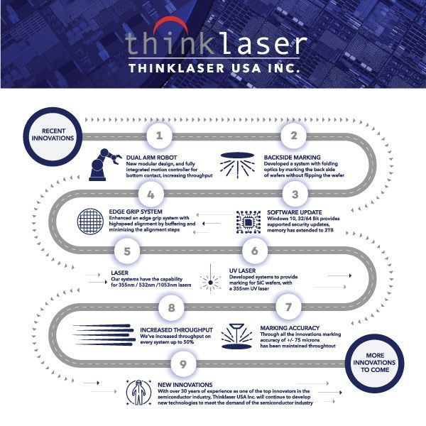
One of the key topics discussed was the evolution of semiconductor materials. As manufacturers increasingly adopt advanced substrates such as silicon carbide (SiC) and gallium nitride (GaN), wafer identification technologies must continue to evolve alongside them. At Thinklaser USA, we are focused on developing solutions that meet the unique challenges presented by these next-generation materials.
The article also explored the history and continued development of the WaferMark® product line. Building on decades of industry experience, our team continues to enhance wafer marking technology to support the growing demands of modern semiconductor fabrication facilities.
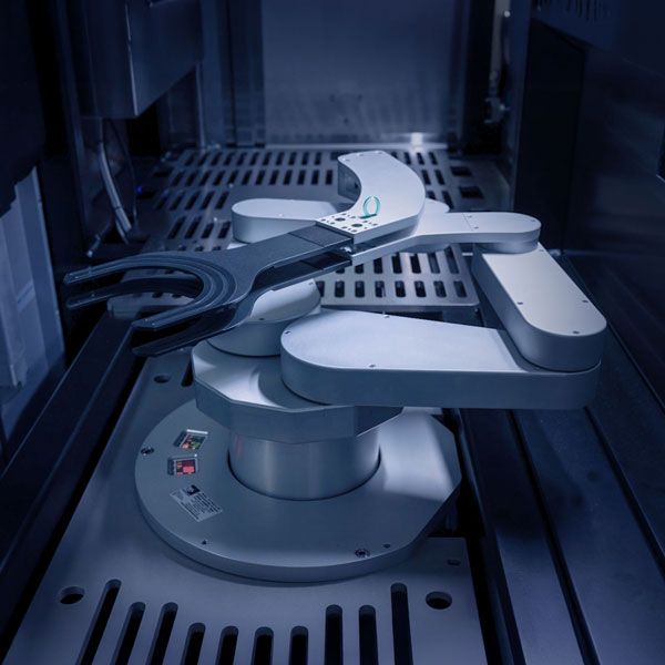
Another important takeaway from the discussion was the increasing importance of automation. Semiconductor manufacturers are under constant pressure to improve throughput while maintaining precision and quality. Our focus remains on delivering reliable, high-performance systems that help customers achieve both objectives.
We appreciate Semiconductor Review for the opportunity to share our story and discuss the future of wafer marking technology. As the semiconductor industry continues to innovate, Thinklaser USA remains committed to providing the expertise, technology, and customer support needed to help manufacturers succeed.
To read the full feature, visit the Semiconductor Review article highlighting Thinklaser USA and Chris Anthony.