
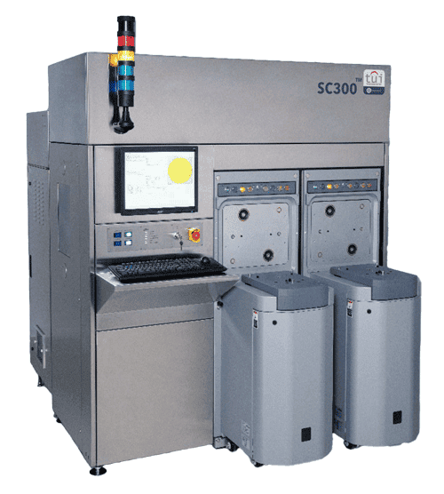
Debris-Free Laser Wafer Marking
THE INDUSTRY-LEADING SOFTMARK SOLUTION
The SC300’s Class 1 cleanroom compatibility and ultra-stable patented diode-pumped laser has helped to make it the industry-leading solution for cost-efficient, highly-readable soft marking of 300 mm wafers for identification and traceability.
PATENTED SUPERSOFTMARK® TECHNOLOGY
The SC300’s proprietary SuperSoftMark® technology, along with its patented diode-pumped laser, enables it to deliver debris-free soft marking, and allows the system to be installed in customer cleanrooms for high-volume production.
HIGH PERFORMANCE WITH GREATER CONTROL
The SC300 combines a high-performance laser system with best-in-class system-level closed-loop control and automated system data logging. All laser performance data is accurately logged to SPC levels of mark quality.
SEMI-COMPLIANT WAFER MARKING
TUI’s WaferMark® systems are fully compliant with SEMI standards for wafer marking: T7, M12 and M13. The SC300 can place multiple mark groups at any orientation on the wafer surface, within a 25 mm band around the wafer’s circumference.
System Specifications
PERFORMANCE
REQUIREMENTS
(STANDARD)
(straight line or arc marking)
SuperSoftMark® Process 0.02 particles/cm, 0.17 particle size measured over 5 mm area
Dot Diameter 50-70 μm +/- 10%
Dot Depth 2.4 μm +/- 0.4 μm
Throughput 125-180 wph, single pulse, 5x9 dot matrix, 12 characters
Material Polished, non-coated, pure Si wafers
Process Vacuum 20 Hg to 25 Hg. 3/8 in diameter press-lock connection
Mark Point Exhaust 20 CFM (560 I/min) flow rate max
2 in (50.8 mm) diameter port
Air-Cooled System Temp: 12.8 – 27 °C (55-80 °F)
(1981.2 mm x 1641 mm x 1204 mm)
Weight EFEM: 1480 lb (671 kg)
Mark Enclosure: 1145 lbs (519 kg)
• 10x18 Double Density Dot Matrix
• 5x9 SEMI Single Density Dot Matrix
• T1 SEMI Specs BC-412 Bar Code
• T7 2D Data Matrix
• Checksum Function (user selectable)
• Custom Fonts Available
Mark Char 80 char/group max
50x50 mm after wafer aligned
Mark Location
Within a 25 mm band around wafer circumference
+/- 75 μm in X & Y relative to primary fiducial
Character Formation
SEMI M12/M13
ISO Class 2 mini-environment
200 mm bridge capability (optional)
Alignment Optical high-resolution wafer aligner
• Windows 10, 32/64 Bit
• DDR3 ECC Memory
• PCI; PCIe x1; PCIe x16 slots
• 10/100/1000 T LAN Ports
• USB 3.0; USB 2.0 Ports
• RS232 ports - Includes Adapter Plates
• Intel 2.5 in Solid State Drives
• 2-Drawer drive carrier for 2.5 in drives
• DVD/DL Drive
TEM00Nd: YLF diode-pumped laser
Wavelength 1053 nm
Optics Flat field focusing lens
Depth 2.4 μm to 5.0 μm
• Menu-driven “fill in the blank” software
• Multiple job file storage capability
• Fault and error logging capabilities
• System diagnostic indicators displayed on
front panel and electronic console
• SECS II/GEM interface
• Four color programmable signal tower
SEMI S2, S8, S14